Features of HDI PCBs
As the digital world becomes increasingly complex, the hardware associated with it must keep getting smaller. This is where HDI PCBs come in, with their more compact size and enhanced signal integrity enabling devices to be slimmer and lighter. This technology is essential for mobile devices, medical equipment like pacemakers and miniaturized cameras, automotive and aerospace products, as well as a variety of consumer electronics.
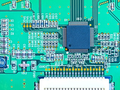
High-density interlayer connections are a key feature of hdi pcb, allowing circuit designs to be more compact and provide greater electrical performance than conventional PCBs. These features can help to reduce production costs, improve design flexibility, and shorten time to market.
HDI PCBs utilize a more efficient design and manufacturing process, requiring fewer layers and smaller components than standard PCBs to achieve the same routing density. This allows for more complex designs to be fabricated with shorter lead times, and can enable new, innovative applications to be realized.
Key Features of HDI PCBs
A key feature of HDI PCBs is the use of microvias, which allow for higher-density interconnection between layers. These microvias have a lower aspect ratio than traditional through holes, making them more reliable and easy to route. The lower aspect ratio also helps to increase the number of available routing channels, enabling high-density connections in areas traditionally reserved for solder pads.
In order to implement these high-density interconnections, the PCB manufacturer must first prepare a stack-up by etching and de-laminating the copper layers. The layers are then stacked together and partially cured before being exposed to heat, which liquifies the prepreg layers and sticks them together. A via formation process then forms the required holes for interconnections between the layers. This can include blind and buried vias, as well as filled plated microvias.
The resulting microvias are then plated with copper and the blind and buried vias are filled, forming a conductive path. The buried vias are then drilled through the core layer and metalized to connect the inner and outer layers.
To achieve the high-density interconnections required by HDI PCBs, the designer will typically hit the limit of what can be mechanically drilled through the core layer. This limits the amount of copper that can be plated through the hole. To increase the copper plating coverage, the designer will use a technique called “via-in-pad.” Once all the vias are formed and plated, the top and bottom layers of the PCB are laminated together, and the edges are trimmed and soldered. The PCB is then ready for testing, evaluation, and shipping.
As the demand for compact and lightweight devices continues to rise, HDI technology will continue to play an important role in meeting those demands. The availability of advanced dielectric materials will further advance the capabilities of HDI PCBs, enabling them to support more sophisticated applications and offer greater thermal and electrical performance. In addition, advances in PCB assembly technologies will further improve the speed and reliability of these high-performance boards. Ultimately, the combination of these factors will create an even more powerful PCB that will meet today’s and tomorrow’s demanding electronic needs.